
Swept-Frequency Source & Fiber-Optic Routing
A high-speed swept-frequency laser varies its output wavelength or frequency. Fiber-optic splitters, couplers, and circulators route the light to the reference path and the sample.
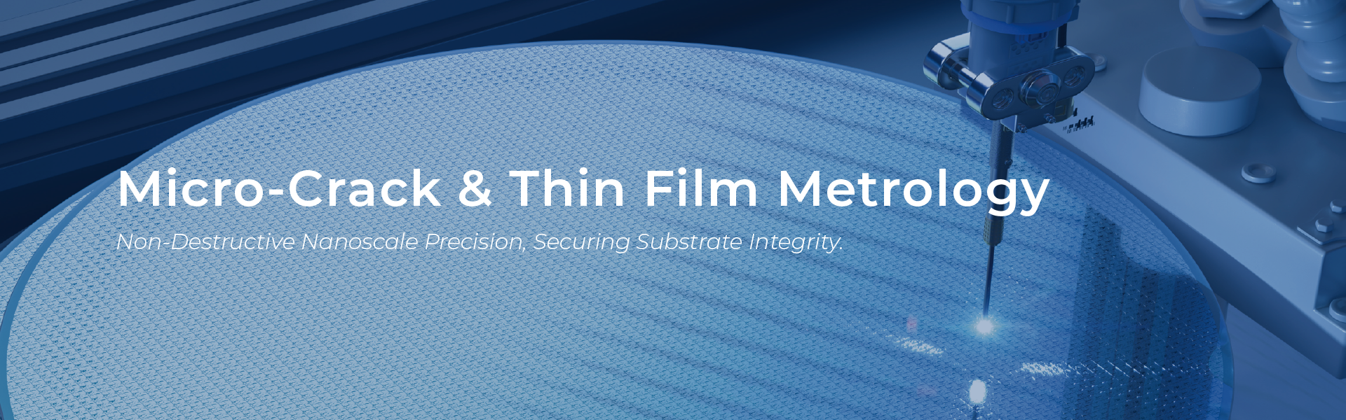

The ILORA-2000 intelligent laser reflectometry analyzer utilizes non-contact optical reflection signals to measure thin film thickness, cavity depth, surface profile, and structural variations, making it ideal for rapid inspection and process quality analysis of wafers, MEMS, packaging substrates, and microstructures.
ILORA-2000 uses high-speed swept-frequency interferometric reflectometry to analyze reflections from material surfaces, thin-film interfaces, and internal structures without physical contact or sample damage. The system combines thickness measurement, structural imaging, and subsurface defect inspection to support R&D characterization, process monitoring, and automated inspection.
Optical path difference information encoded in the interference signal is converted into a depth-resolved reflectivity profile, producing a single-point A-scan. Line and area scanning then reconstruct 2D cross-sectional and 3D structural images to characterize material layers, interface positions, and structural anomalies.
A swept-frequency laser rapidly scans a defined wavelength or frequency range. Reflections from different sample interfaces interfere with the reference light. Photodetection and digital signal processing extract depth information for each interface.
A high-speed swept-frequency laser varies its output wavelength or frequency. Fiber-optic splitters, couplers, and circulators route the light to the reference path and the sample.
Light reflected from material surfaces, thin films, adhesive layers, and internal structures interferes with the reference light. Balanced or I/Q detection captures the resulting interference signals.
An ADC digitizes the detected signals. FPGA/DSP processing performs calibration, filtering, and depth conversion to generate a depth-resolved reflectivity profile.
Each point measurement produces an A-scan. Line and area scans reconstruct 2D cross-sections and 3D structures for thickness, interface, and defect analysis.
Integrates a swept-frequency source, photodetection, and digital processing to convert interference signals from multiple interfaces into depth information, supporting non-contact scanning and structural analysis.
Combines depth measurement with scanning to characterize surface topography, thickness distribution, and thin-film and adhesive-layer interfaces, while helping identify cracks, bubbles, and other subsurface structural anomalies.
The supplied comparison shows narrower reflection peaks for ILORA-2000, which can help distinguish adjacent interfaces. Measurement performance is reported separately in terms of thickness measurement error, repeatability, and multipoint standard deviation.
Comparison Note | The peak-shape comparison applies only to the supplied illustration and its measurement conditions. It does not establish a universal performance comparison across all materials or OCT systems. Interface resolution, thickness measurement error, and repeatability are distinct metrics and should not be used interchangeably.
Measures wafers, thin films, ABF/RDL dielectric layers, adhesive layers, and multilayer materials to evaluate thickness and spatial distribution.
Analyzes surface topography, flatness, warpage, grooves, and etch depth to support dimensional characterization and surface quality assessment.
Examines thin-film interfaces, bonding interfaces, internal layer structures, and adhesive distribution to assess multilayer structures and bond condition.
Uses reflection signals and structural images to identify microcracks, fractures, bubbles, voids, delamination, and other optical discontinuities.
Application Note | Accessible depths, interfaces, and detectable defects require validation for the material's optical properties, layer structure, and measurement configuration.
The following results are compiled from the supplied data and separately describe measurement error, repeatability, and multipoint measurement standard deviation.
< 0.1 µm
Thickness measurement error reported in the supplied data.
Approx. 0.03 µm
Repeatability expressed as 3σ.
< 100 nm
Standard deviation of multipoint thickness measurements reported in the supplied data.
Data Interpretation | These values should not be interpreted as axial resolution, minimum measurable film thickness, or minimum detectable crack size. The ABF multipoint standard deviation is also not equivalent to repeatability at a single location. Sample conditions, calibration procedures, sampling methods, and test conditions should be confirmed for each application.
The ILORA-2000 series includes entry-level, high-speed, advanced, and flagship models. The reported frequency values and product tiers are listed below.
| Model | Frequency* | Product Tier |
|---|---|---|
| ILORA-2000-B | 20–100 Hz | Entry-Level |
| ILORA-2000-HS | 1,250–2,500 Hz | High-Speed |
| ILORA-2000-UHS | > 200,000 Hz | Advanced |
| ILORA-2000-EHS | > 10 MHz | Flagship |
Scroll horizontally to view all columns if needed ↔
*Frequency values are reproduced from the supplied image. The source does not specify whether they represent sweep frequency, A-scan rate, or another system parameter. They are therefore listed as “Frequency” and should not be interpreted directly as complete 2D/3D imaging rates. Refer to the manufacturer's latest datasheet for parameter definitions and applicable operating conditions.
Under non-contact and non-destructive conditions, ILORA-2000 simultaneously retrieves thickness, surface topography, interface, and defect data, making it suitable for R&D laboratories, in-line process stations, and automated inspection systems.
Silicon wafer ground thickness, parallelism, warpage, and single/multilayer thin-film coating uniformity.
Front and back multi-point thickness distribution, subtle uniformity variations, internal interfaces, and local anomalies.
Non-contact monitoring of etch depth, remaining silicon thickness, trench structures, and process variations.
Adhesive layers, underfill materials, epoxy, bonding interfaces, voids, air bubbles, and delamination.
Post-dicing micro-cracks, fractures, film non-uniformities, internal anomalies, and hidden structural defects.
Conceptual inspection of backside power delivery networks (BSPDN), Chiplet/3D stacking, and advanced packaging interfaces.
Fiber-guided miniaturized sensing heads enable the integration of measurement optical paths into space-constrained equipment stations. Combined with high-speed scanning stages, ADCs, and real-time FPGA/DSP processing, the system supports high-speed sampling, measurement logging, and seamless process tool integration.