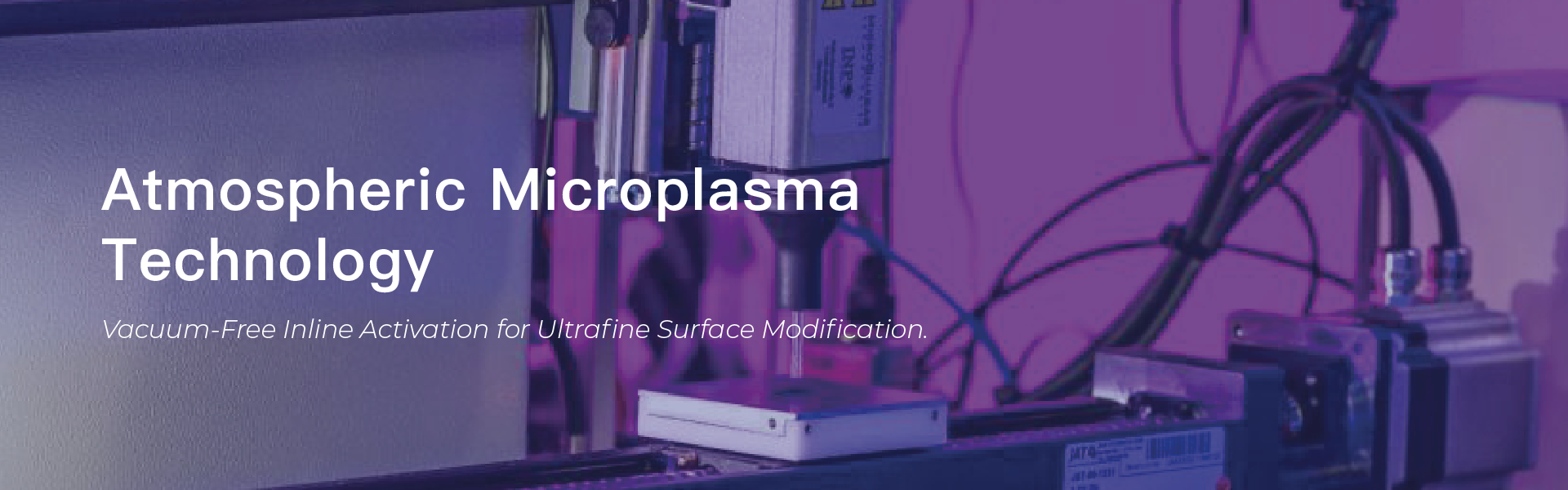
The Micro Plasma atmospheric microplasma system enables localized surface cleaning, activation, and surface energy tuning to enhance liquid wettability, adhesion, and coating uniformity, making it ideal for underfill, precision dispensing, package bonding, and microfluidic processes.
MicroQuasar SurfAP3® reduces the plasma-processing line width to approximately 30 μm. A miniaturized plasma source generates highly concentrated active ions, electrons, and free radicals. Combined with a precision nozzle, controlled gas flow, and stable energy delivery, the system follows digital paths to create straight lines, curves, and complex patterns.
The process requires no photomask, stencil, or custom electrode, helping reduce tooling costs and product changeover time while supporting both high-mix, low-volume production and scalable manufacturing.
Surface
Activation & modification
Micro Plasma Surface Activation and Modification
By adjusting plasma power, reactive gases, nozzle distance, scanning speed, treatment passes, and path overlap, Micro Plasma can precisely modify surface energy, chemical functional groups, wettability, and adhesion. It is applicable to metals, silicon wafers, glass, ceramics, polymers, fibers, and other materials. Beyond precision cleaning and surface activation, the process can also support microscale thin-film removal, micro/nanotexture formation, and selective deposition of functional materials.
System
Integrated platform
Integrated Hybrid Surface-Engineering Platform
MOL can integrate MicroQuasar microplasma, a precision XY stage, vision alignment, laser microstructuring, functional-material deposition, and real-time process monitoring into a hybrid surface-engineering platform comprising laser microstructuring, localized 30 μm plasma activation, selective coating or dispensing, and inline quality inspection. The laser establishes micro/nanoscale geometries, while Micro Plasma adjusts surface chemistry and interfacial functionality, enabling coordinated control of material structure, surface energy, wettability, and adhesion.
Micro Plasma Applications in Semiconductors and Microelectronics
With localized processing capability down to 30 μm, Micro Plasma is particularly well suited to advanced semiconductor packaging and microelectronics manufacturing. In Hybrid Bonding and TCB processes, it can selectively clean and activate Cu pads, micro-bumps, and bonding interfaces to increase surface energy, solder wettability, and bond strength while minimizing impact on adjacent passivation, low-k materials, and sensitive structures. In RDL processes, patterned activation can be applied to Cu, PI, PBO, and ABF interfaces to improve adhesion between metals and dielectric materials, while also supporting cleaning around vias, pretreatment before seed-layer deposition, and localized film trimming.
FLUID CONTROL & BIOINTERFACES
Precision Dispensing, Microfluidics, and Biointerfaces
In underfill and precision-dispensing processes, Micro Plasma can create high-surface-energy flow paths on a substrate to guide adhesive along predefined directions, accelerate capillary filling, and reduce voids. Boundaries with different wettability can also be formed to keep adhesive away from optical windows, pads, connectors, and other no-overflow areas. The same capability is suitable for microfluidics, biochips, and biosensors, including microchannel hydrophilization, droplet guidance, reaction-zone functionalization, and selective immobilization of biomolecules.
PHOTONICS & OPTICAL PACKAGING
Silicon Photonics and Optical Packaging
For silicon photonics and optical packaging, Micro Plasma can locally clean and activate bonding areas on fiber end faces, V-grooves, FAUs, MLAs, and optical connectors. This improves the wetting uniformity and adhesion reliability of optical adhesives while reducing the risk of residue, bubbles, and unintended treatment of non-target optical surfaces. Combined with high-precision vision alignment, the processing path can be corrected automatically according to the actual component position.
INTEGRATED SURFACE ENGINEERING PLATFORM
This integrated platform supports ABF and RDL interface enhancement, Hybrid Bonding, TCB, underfill flow-path control, SiC microchannel functionalization, fiber and FAU bonding, and functional-film deposition for sensors. It provides semiconductor, optoelectronics, biomedical, and advanced-material industries with an advanced surface-engineering solution combining high resolution, maskless processing, low thermal impact, broad material compatibility, and scalable manufacturing.